GAIA is an ambitious EIC Pathfinder project pioneering a completely new paradigm for the Internet of Things: biodegradable, battery-less, and seamlessly integrated microelectronic systems that communicate using ambient cellular infrastructure. Our long-term vision is a world where digital services blend into materials and objects naturally — without batteries, without electronic waste, and without the need for proprietary networks..
A New Class of Sustainable Microelectronics
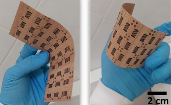
GAIA builds on breakthroughs in biodegradable materials, transient electronics, antenna-based sensing, and ambient backscatter communication to create the first generation of fully transient IoT devices. These devices operate with ultra-low power, extract energy from surrounding RF signals, and naturally degrade at the end of their life cycle. By embedding intelligence directly into everyday objects — from packaging to logistics and healthcare products — GAIA envisions a circular, infrastructure-aligned, and maintenance-free IoT ecosystem.
Co-Design Across Materials, Electronics & Networks
GAIA follows a holistic co-design approach spanning materials, circuits, antennas, and cellular networking:
Advanced bio-based substrates optimized for RF performance
Transient system-on-chip architectures integrating sensing, processing, and wireless backscatter
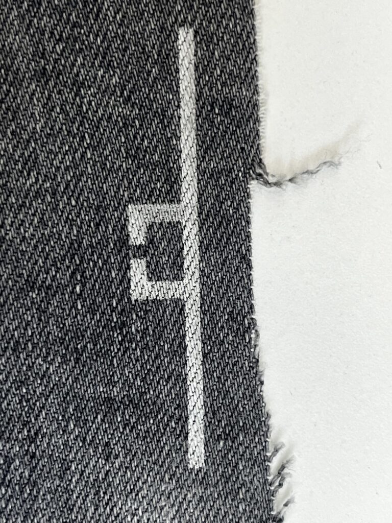
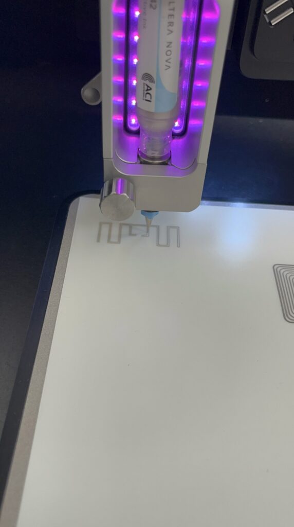
Printed antennas engineered for efficiency on organic surfaces
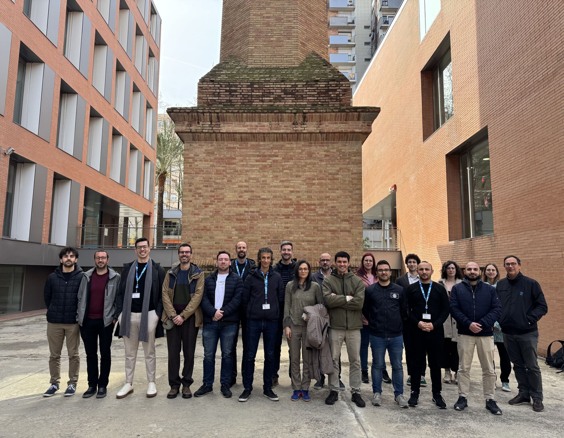
Last week GAIA partners meet in Barcelona for the kickoff meeting of the project. The meeting was hosted by the project coordinator Xavier Vilajosana at the Universitat Oberta de Catalunya (UOC). During 10-11th of March, the partners discussed the objectives, scientific vision and ambition, work plan, and collaboration strategies. This meeting established the foundations for…
The GAIA project officially started on February 2026! GAIA reimagines the Internet of Things (IoT) by leveraging breakthroughs in biodegradable electronics and ambient communication to deliver a transformative vision: a seamless, sustainable, and circular IoT ecosystem. It introduces a new class of transient, ultralow-power microelectronic systems that combine sensing, computation, and communication in a single…
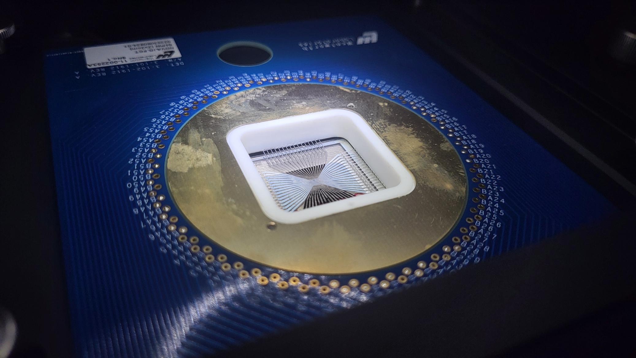
Biodegradable & Transient Electronics GAIA develops microelectronic systems made from bio-based materials such as chitosan, cellulose, and transient metals. These components — processors, sensors, antennas and interconnects — are designed to function for a limited time and then safely decompose, eliminating e-waste.
Ambient Backscatter Communication Instead of generating their own radio signals, GAIA devices reflect and modulate existing cellular transmissions. This enables battery-free communication at extremely low power, compatible with emerging 5G/6G infrastructures.
Wake-on-Sensor Intelligence Novel material-based triggering mechanisms allow GAIA devices to remain dormant indefinitely and activate only when needed — for example, upon detecting a temperature threshold in a cold-chain package.
Edge-Assisted Computing Minimal local processing is combined with edge/cloud intelligence, enabling sustainable AI services even with ultra-simple hardware. This hybrid approach redefines how we design and distribute intelligence across IoT systems.
The Partners
University Oberta de Catalunya (UOC) – Spain
Role: Project Coordinator • Lead in Backscatter Communication, Cellular Protocols & Edge Architecture UOC pioneers ultra-low-power wireless systems, cellular backscatter, and antenna-based sensing. As coordinator, UOC leads the GAIA architecture, illumination protocols for 5G/6G ambient IoT, and integration with edge/cloud systems. Its research shapes the project’s network-centric approach and overall vision for sustainable IoT.
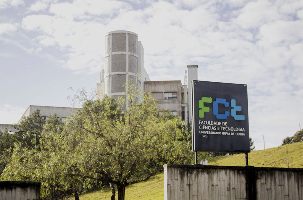
FCT NOVA (NOVA) – Portugal
Role: Lead in Biodegradable Materials & Transient ElectronicsNOVA develops the biodegradable substrates, interconnects, and semiconductor materials at the core of GAIA’s transient electronic systems. Their expertise spans 2D materials, MXenes, ZTO-based devices, printed electronics, and fabrication techniques that enable transient VLSI and biodegradable memristive architectures.
Institut National de Recherche en Informatique et en Automatique (INRIA) – France
Role: Lead in Transient SoC Design & Integration INRIA drives the development of GAIA’s transient system-on-chip, integrating sensing, processing, and cellular backscatter interfaces. Building on their SCuM and ultra-low-power RISC-V architectures, INRIA leads SoC design, modeling, co-simulation, and interfacing with biodegradable reservoirs and antennas.
Technische Universität Braunschweig (TUBS) – Germany
Role: Lead in Printed Electronics, Sensing & Wake-On Activation TUBS specializes in hybrid microelectronics, sensor-triggered activation, and printed biodegradable interconnects. Their work enables GAIA’s wake-on-sensor mechanisms, ultra-low-power triggering, and robust integration between CMOS/transient electronics and biomaterial-based substrates.
Tampere University (TAU) – Finland
Role: Lead in Antenna Design, Printed RF Components & Biodegradable Sensing TAU develops GAIA’s printed antennas, carbon-based conductive inks, and RF-ready biodegradable substrates. Their expertise in flexible and organic RF components ensures efficient backscatter communication and antenna-based sensing despite the constraints of transient materials.
Centre Tecnològic de Telecomunicacions de Catalunya (CTTC) – Spain
Role: Lead in 5G/6G Integration, Illumination Protocols & Edge-AI CTTC brings deep expertise in 5G/6G radio systems, O-RAN networks, and edge compute architectures. They lead validation within real cellular infrastructure, design backscatter-compatible illumination strategies, and develop MEC-based inference pipelines that enable GAIA’s distributed AI-enabled sensing.
This project has received funding from the European Union’s Horizon Europe research and innovation programme under grant agreement No 101256099. Views and opinions expressed are however those of the author(s) only and do not necessarily reflect those of the European Union or European Innovation Council and SMEs Executive Agency (EISMEA). Neither the European Union nor the granting authority can be held responsible for them.